Chilling Out for Super Solar: How Cryo-Cool CdS Films Could Revolutionize Your Panels!
Hey everyone! Ever stop to think about the unsung heroes inside those solar panels soaking up the sun? One crucial little component is the “optical window,” and for that job, Cadmium Sulfide (CdS) is a pretty popular kid on the block. It’s got some great properties that help solar cells do their thing. But here’s the rub: making these CdS layers super thin, super smooth, and super effective isn’t as easy as just slapping some material down. It’s a delicate dance of physics and chemistry!
We’ve been diving deep into this, trying to figure out the absolute best way to create these CdS thin films. And let me tell you, we’ve stumbled upon some seriously cool findings – literally! We’re talking about comparing the old-school “classical” methods with a newer, “cryogenic” approach. The big question: can chilling things out lead to better solar cell performance? Spoiler: it looks promising!
Why All the Fuss About CdS Thin Films?
So, why CdS? Well, its forbidden energy gap (around 2.45 eV, for the geeks out there) is just right for letting a good chunk of sunlight pass through to the active layer of a solar cell, where the magic of converting light to electricity happens. Think of it as the perfect bouncer for a nightclub – letting the right “wavelengths” in and keeping others out. Plus, CdS films naturally grow as n-type semiconductors, which is handy for building the necessary electronic structures in solar cells.
Now, the thickness of this CdS window layer is a big deal. If it’s too thick, it can block some of the valuable blue light from reaching the part of the cell that needs it. This means less current, and nobody wants that! Studies suggest an optimal thickness is around 100-150 nanometers. That’s incredibly thin – we’re talking thinner than a strand of your hair! Producing such a nano-sized layer that’s also homogeneous (uniform everywhere) and doesn’t have tiny holes (porosity) is a real challenge with traditional methods like chemical bath deposition or standard vacuum evaporation. Sure, fancy techniques like Atomic Layer Deposition (ALD) or Pulsed Laser Deposition (PLD) can do a good job, but they often come with hefty price tags, can be slow, and aren’t always easy to scale up for mass production of large solar panels. We needed something better, potentially simpler, and more economical.
The Showdown: Classical Warmth vs. Cryogenic Chill
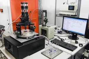
This is where our big experiment comes in. We decided to produce CdS thin films using two distinct thermal evaporation techniques within a quasi-closed volume.
- The classical technique (let’s call it the “hot” method): Here, we deposited CdS onto substrates heated to 373 K, 473 K, and 573 K (that’s 100°C, 200°C, and 300°C).
- The cryogenic technique (our “cold” contender): For this, we cooled the substrates right down, working in 50 K steps from a frosty 100 K up to 300 K (-173°C to 27°C).
The idea behind the cryogenic method is that low temperatures can reduce how much atoms and clusters move around on the surface (surface diffusion) as the film is forming. This can lead to smaller particle sizes and, potentially, higher quality films. We were particularly interested in a phenomenon called the “soliton wave model” that might kick in at these low temperatures, leading to some pretty unique film growth.
We used high-purity CdS powder and carefully controlled the distance between our source material and the substrate to keep temperature fluctuations minimal. For the cryogenic setup, we had a neat system with a substrate cooling section (using liquid nitrogen, brrr!) and a quartz reactor chamber to create a saturated vapor of CdS. Once the substrate hit the target cold temperature, we’d let the vapor interact with it for about 15 minutes to grow our film. Then, it was time for the exciting part: characterization!

What Did We See? Structure, Structure, Structure!
The first thing we looked at was the crystal structure using X-Ray Diffraction (XRD). Good news all around: all our films, whether hot or cold grown, showed a hexagonal structure and preferred to grow along the (002) plane. This is the crystal orientation we want for CdS in these applications. However, we noticed something really interesting: the film produced at 200 K (-73°C) using the cryogenic technique showed a particularly strong reflection from this (002) plane. This suggests the crystal structure was becoming more like a single crystal – super orderly! On the flip side, the film made at 473 K (200°C) with the classical method seemed to have the highest overall crystallization rate.
But the real jaw-dropper came when we looked at the films under a Field Emission Scanning Electron Microscope (FESEM). For most temperatures (250 K to 573 K), the films grew by what’s called an “island growth mechanism” – imagine little islands of material forming and then merging, leading to grains of different sizes and shapes. But at 200 K with the cryogenic technique, it was a whole different story! The film was made up of these beautiful, equally sized spherical grains. This is a tell-tale sign of the soliton growth mechanism we were hoping to see!
What’s this soliton thing, you ask? Imagine tiny, perfectly sized clusters of CdS forming in the vapor. When these “critically sized neutral clusters” hit the super-cooled substrate, they don’t just stick; they create these special “soliton waves” on the surface. These waves allow the clusters to glide across the substrate without losing energy, almost like tiny surfers. Because they’re neutral and just the right size, they pack together incredibly tightly and uniformly. This leads to a homogeneous surface and a very consistent thickness. It’s like building a wall with perfectly identical, perfectly placed bricks versus a jumble of different-sized stones. Our previous work with gold and CdTe thin films using cryogenic methods also showed this awesome soliton growth, so we were thrilled to see it with CdS!
We also used an Atomic Force Microscope (AFM) to get a 3D look at the surface roughness. And guess what? The CdS thin film produced at that magic 200 K substrate temperature had the smallest average surface roughness value (Ra) – a mere 1.047 nanometers! That’s incredibly smooth. For comparison, CdS films made by conventional vacuum methods often have roughness values between 25-45 nm. Smoothness is vital because a rough interface between the CdS window layer and the absorber layer in a solar cell can lead to all sorts of problems, like recombination losses, which sap efficiency.
Letting the Sunshine In: Optical Performance
Okay, so our 200 K cryogenic film looks amazing structurally, but how does it perform as an optical window? We zapped our films with light across a range of wavelengths (300-1000 nm) to measure their optical transmittance. The results were clear: while most films were pretty similar at higher wavelengths, in the crucial low wavelength region (like blue light), the samples made with the cryogenic method, especially the 200 K one, showed significantly higher transmittance! This is fantastic news because it means more of that high-energy light can get through to the active layer of the solar cell, potentially boosting the current it can produce.
We also calculated the energy band gap (Eg) from this data. We found that Eg generally increased as the substrate temperature decreased, ranging from 2.37 eV for the hottest film (573 K) to 2.47 eV for the coldest (100 K). Our star performer, the 200 K film, clocked in at a very respectable 2.43 eV. This shift in band gap can be due to a mix of factors like grain size, carrier density, and internal stress in the film. It seems the smaller grain sizes at lower temperatures play a big role here. Importantly, we didn’t see signs of quantum confinement effects, which usually only pop up with even tinier grains (less than 5 nm).

The Nitty-Gritty: Composition and Electricals
What about the actual ingredients? We used Energy Dispersive Spectroscopy (EDS) to check the chemical composition – specifically, the ratio of Cadmium (Cd) to Sulfur (S). Ideally, you want a perfect 1:1 ratio (stoichiometric). We found that the films produced at 200 K (cryogenic) and 473 K (classical) were the closest to this ideal. Other temperatures showed slight deviations, often being a bit rich in Sulfur. Stoichiometry is super important for the film’s electrical and optical properties, so hitting that sweet spot is key.
Now for the electrical properties. We measured resistivity and carrier concentration. As the substrate temperature went down (and grain size decreased), the resistivity of the CdS films tended to increase (from 1.25 × 10³ Ω-cm at 573 K to 5.39 × 10³ Ω-cm at 100 K). Conversely, the carrier concentration decreased (from 3.91 × 10¹⁷ cm⁻³ to 1.73 × 10¹⁶ cm⁻³). Our 200 K cryogenic film showed a resistivity of 3.39 × 10³ Ω-cm and a carrier mobility of 48.8 × 10⁻³ cm²/V·s. While commercial-grade films might aim for slightly lower resistivity and higher mobility, the other amazing properties of our 200 K film – its high transmittance, low roughness, and good stoichiometry – are expected to more than compensate, leading to better overall device performance by improving the interface quality and reducing recombination losses. It’s all about the complete package!
To make sure our electrical measurements were sound, we used Indium (In) for our ohmic contacts. We even etched the CdS surface beforehand to remove any pesky oxides. The contact resistance we got was around 1.8 Ω cm², which is nice and low, meaning we weren’t losing much signal at the contacts.
Shining a Light on Defects: Photoluminescence Insights
Finally, we used Photoluminescence (PL) to get a handle on the defects within the crystal structure. Defects like vacancies or impurities can really mess with a semiconductor’s performance. We excited the films with UV light and looked at the light they emitted in response. The PL spectra can tell you a lot about the types and amounts of defects present.
The main emission peak for CdS is usually a green one, related to near-band-edge recombination. But we also looked for other emissions – blue, orange, and red – which are often linked to specific defects. Here’s the exciting part: the CdS samples prepared at cryogenic temperatures (especially 200 K and below) showed significantly suppressed emissions from these defect-related peaks! This is strong evidence that these cryogenically grown films have better surface quality and fewer structural gremlins. Fewer defects mean a happier, more efficient solar cell!

So, What’s the Big Takeaway?
After all this poking and prodding, it’s pretty clear that how you make your CdS thin films matters – a lot! Here’s a quick rundown of what we learned:
- All our films, hot or cold, grew in the desired hexagonal structure.
- The real magic happened at 200 K using the cryogenic technique, where we saw the soliton growth mechanism in action. This gave us films with incredibly uniform, nano-sized spherical grains.
- This 200 K film also boasted the lowest average surface roughness (a super-smooth 1.047 nm) and the highest optical transmittance, especially for that important blue light.
- It also had a near-perfect stoichiometric (Cd/S) ratio.
- Electrically, while its resistivity was a bit higher than some, its overall package of superior structural and optical properties, plus fewer defects (as shown by PL), makes it a fantastic candidate.
- Generally, as we cooled the substrate, the grain size decreased, which led to an increase in resistivity and the energy band gap.
- Photoluminescence confirmed that films grown at cryogenic temperatures (≤ 200 K) had fewer defects.
In a nutshell, we’ve pinpointed that producing CdS thin films at a substrate temperature of 200 K using our new cryogenic technique could lead to some serious improvements in solar cell efficiency. These films are smoother, more transparent where it counts, more structurally sound, and have fewer pesky defects. It just goes to show that sometimes, to make things better, you just need to chill out a bit! We’re really excited about what this could mean for the future of photodevices.
Source: Springer