Peeking at Tiny Electrons: How We’re Using Cold and Light to Unlock Material Secrets!
Hey there, fellow science enthusiasts! Ever wonder what’s happening at the truly, truly tiny scale in those fancy new materials everyone’s talking about? I’m talking about systems where electrons are squished into super-thin, 2D layers – think of them as electron pancakes! These “confined electron systems,” like 2D electron gases (we call ‘em 2DEGs for short), nifty 2D materials like graphene, or even mind-bending topological insulators, are packed with promise for future tech. Imagine faster computers, super-efficient energy devices, you name it. But, there’s a catch: these materials can be a bit… finicky. They’re super sensitive to tiny imperfections, or defects, which can create nanoscale messy spots, or inhomogeneities. And honestly, figuring out *why* these spots form has been a bit of a head-scratcher.
Now, we’ve got a cool tool in our arsenal called scattering-type scanning near-field optical microscopy, or s-SNOM for those of us who like to save our breath. It’s brilliant because it lets us peek at these buried electron systems without wrecking them, and with amazing nanoscale detail. Think of it like having super-powered nano-vision! The problem was, even with s-SNOM, it was like looking at a blurry picture where two important details – how many charge carriers (like electrons) there are, and how easily they can zip around (that’s their mobility) – were all muddled together. We just couldn’t clearly tell them apart.
A “Fingerprint” Breakthrough at Chilly Temperatures
But guess what? We’ve had a bit of an “aha!” moment. We figured out, and then proved, that for a classic 2DEG system – the one that forms at the interface of LaAlO3 (LAO) and SrTiO3 (STO) – there’s a special “fingerprint” in its optical response. This fingerprint was hiding in a spectral region that was previously super hard to see. To catch it, we had to get creative. We took our s-SNOM setup, chilled it down to a frosty 8 Kelvin (that’s about -265 degrees Celsius or -445 Fahrenheit – brrr!), and zapped it with a state-of-the-art, tunable narrow-band laser in the mid-infrared range. This laser is a real gem because it’s bright and clean in just the right spot to see this fingerprint.
Why all the fuss about LAO/STO? Well, this interface between two insulators magically becomes metallic, hosting a 2DEG! It’s a fantastic playground for studying high-concentration, correlated electron systems where electrons really interact with each other, leading to cool stuff like superconductivity and magnetism not found in the parent materials. But, as I said, understanding how this 2DEG forms locally and how defects mess with it has been tricky.
Previous s-SNOM studies on LAO/STO were a bit indirect. They’d look at how the 2DEG dampened vibrations (phonons) in the STO substrate or showed up as a sort of constant background signal at higher frequencies. But directly mapping the local charge carrier density and mobility? Tough luck, because their effects on the spectra could cancel each other out. Our new “fingerprint” method changes the game. It’s a specific pattern in the near-field spectrum that lets us untangle the influences of carrier concentration and mobility. It’s like finally getting separate volume and tone knobs for the electron orchestra!
How We Spot the Fingerprint
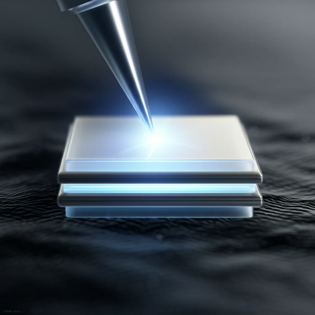
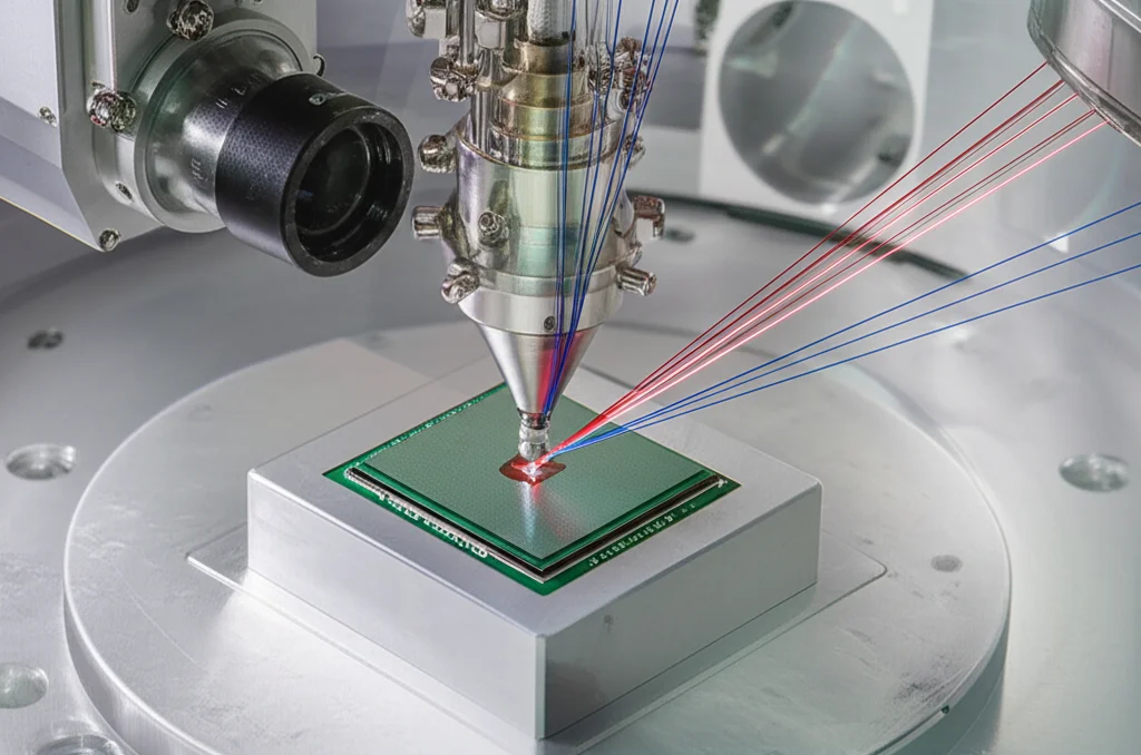
So, how does this s-SNOM wizardry work? Imagine a super-sharp metal-coated atomic force microscope (AFM) tip, scanning across our LAO/STO sample. This tip is tapping up and down very quickly. We shine our special laser onto this tip. The tip acts like a tiny antenna, creating intense “near-fields” right at its apex. These fields interact with the sample, and the light that scatters back is collected. Because the interaction is so localized to the tip, we get that sweet nanoscale resolution, way better than what the wavelength of light would normally allow.
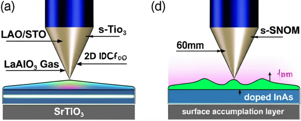
To get clean, meaningful data, we use a clever trick called pseudo-heterodyne interferometric detection, which lets us separate the signal into amplitude and phase. And, because the absolute signal can depend on nitty-gritty experimental details (like the exact tip shape), we normalize our measurements to a reference sample. For our LAO/STO experiments, we did something even smarter. We compared samples where the STO substrate was prepared slightly differently: one that forms a conducting 2DEG (TiO2-terminated) and one that stays insulating (SrO-terminated after a special treatment). These samples were made from the same STO substrate, just with a tiny tweak to the surface before depositing the 3nm-thin LAO layer. This way, by comparing the s-SNOM signal from the conducting interface to the insulating one, we can really isolate the 2DEG’s contribution. It’s like having a perfect “control” experiment built right in!
When we did this at room temperature, the simulations showed some changes, but it wasn’t super clear. However, at cryogenic temperatures, where the 2DEG mobility gets a boost, things get interesting. Our simulations predicted that if you look at a specific frequency range (roughly 700 to 900 cm-1), and you divide the signal from the 2DEG sample by the signal from the insulating sample, a characteristic pattern with three distinct peaks emerges. That’s our fingerprint! This region was tough to explore before because the overall signal is pretty weak, demanding a laser with a fantastic signal-to-noise ratio – which our new toy thankfully has.
Decoding the Electron Secrets: Concentration vs. Mobility
Now, here’s the really cool part. These three peaks in the fingerprint spectrum don’t just look pretty; they tell us a story. Our models predicted (and our experiments confirmed!) that changes in the 2DEG’s carrier mobility (how easily electrons move) and its carrier concentration (how many electrons there are) affect these peaks differently.
- If you crank up the mobility, the first peak (around 750 cm-1) gets noticeably taller, while the other two don’t change much. But there’s a limit; this effect tends to saturate at higher mobilities (around 80 cm²/Vs in our simulations for LAO/STO).
- If you increase the carrier concentration, all three peaks tend to grow, and this effect is generally stronger and doesn’t saturate as easily in the ranges we looked at.
This difference is golden! It means we can finally look at a local spot on our sample, measure its fingerprint spectrum, and get separate clues about the electron concentration and mobility there. We actually did this! We picked two different spots on our conducting LAO/STO sample, measured their fingerprint spectra at 8K, and voilà – they were different! One spot seemed to have a higher carrier concentration but lower mobility (n2D= 8 × 1013cm-2, µ = 10 cm2/Vs) compared to another (n2D= 6 × 1013cm-2, µ = 20 cm2/Vs). Sometimes, to get the simulations to perfectly match the experimental wiggles, we also had to consider tiny variations in the LAO layer’s properties, perhaps due to strain from cooling. This just shows how sensitive the technique is!
Mapping the Nanoworld’s Bumps and Wiggles
We even did some imaging. We scanned our s-SNOM tip across an area of the sample at a single frequency (700 cm-1, where the signal is strong) and saw significant variations in the near-field signal. Then, we picked a few points along a line in this map and measured the full fingerprint spectrum at each point. Sure enough, the shape of the fingerprint, particularly that first peak, changed as we moved from point to point. Our simulations suggest this was mainly due to the 2DEG mobility varying locally, changing from about 8 cm²/Vs to 40 cm²/Vs. It’s fascinating because it means we can now link those visual “inhomogeneities” in the s-SNOM images to actual, quantifiable changes in local electronic properties. We also noticed that sometimes, just by scanning, we might be subtly changing these properties – something known to happen in LAO/STO at low temperatures due to effects like electrostatic gating from the tip or persistent photoconductivity. Our fingerprint spectroscopy is now a super-sensitive tool to dig into these mysteries.
Why is it So Sensitive? The Magic of Zero-Crossings
You might be wondering, what’s the secret sauce that makes this fingerprint region so sensitive? It turns out that s-SNOM is particularly responsive to tiny changes in a material’s optical properties (its dielectric function, ε) when the real part of this function, Re[ε], is close to zero. It’s like finding the sweet spot on a guitar string that resonates most strongly. Our fingerprint region for LAO/STO is cleverly positioned around such sensitive zones, which are influenced by the material’s phonons (lattice vibrations) and the free electrons of the 2DEG. Adding the 2DEG shifts these optical properties just enough to create those characteristic peaks when we do our special normalization.
Not Just for LAO/STO: A Universal Tool?
And the best part? This isn’t just a one-trick pony for LAO/STO. We believe this “near-field fingerprint spectroscopy” approach is pretty universal. To prove it, we modeled another cool system: doped Indium Arsenide (InAs). Doped InAs is a semiconductor that has a “surface accumulation layer” – basically, a thin layer right at its surface with an even higher concentration of free electrons than the bulk material beneath it. We simulated what the s-SNOM signal would look like. Just like with LAO/STO, if you normalize the signal from InAs *with* its accumulation layer to what it would be *without* it (or with a different bulk doping), you get a fingerprint spectrum with three peaks! Interestingly, for InAs, changing the electron mobility mainly affected the *third* peak, not the first one as in LAO/STO. This shows that while the concept of a fingerprint is general, its specific shape and how it responds to parameters like mobility is unique to the material system and its geometry. This is fantastic because it means we can tailor the analysis for all sorts of confined electron systems.
So, what we’ve cooked up here is a powerful way to use s-SNOM, especially with these new-fangled tunable lasers, to really get under the hood of modern electronic materials. By looking for these “near-field fingerprint spectra,” which we get by cleverly comparing slightly different states or parts of a sample, we can tease out information that was previously all mixed up. For LAO/STO, we can finally get a better handle on local carrier concentration and mobility separately. This is huge for understanding things like defects – maybe a spot where the LAO layer is a bit thinner, or there’s an atomic step, or some missing atoms. And because we’re doing this at low temperatures where mobility is higher, we’re even more sensitive to what’s happening right at that 2DEG interface, potentially even learning about how the electrons are distributed vertically.
The Future is Bright (and Nanoscale!)
Looking ahead, this technique isn’t just for LAO/STO or InAs. We’re excited to point our cryo-s-SNOM and its fingerprinting powers at other fascinating confined electron systems. Think about other oxide interfaces, or those amazing van der Waals heterostructures where you stack different 2D materials like LEGO bricks, or even topological insulators that have those weird conducting surfaces. By getting this kind of spatially resolved information, we can really help design better, more reliable nanoelectronic devices. It’s like having a detailed map and a diagnostic toolkit for the nanoworld, all rolled into one. Pretty neat, huh?
Just a little note on how we make these LAO/STO samples: We use a technique called pulsed laser deposition (PLD) to grow about 3 nanometers (that’s 8 unit cells) of LaAlO3 onto specially prepared SrTiO3 substrates. The growth happens at 800°C in a low oxygen pressure. We can even watch it grow layer by layer! For the s-SNOM, we used a commercial cryo-neaSCOPE from attocube systems, chilled with a closed-cycle cryostat to 8K, and that brilliant EKSPLA laser. The modeling involves some clever physics with the Finite Dipole Model and Transfer Matrix Method to connect what the tip “sees” to the material’s actual properties.
Source: Springer Nature


