Whoosh! These New 2D Materials Have Super-Speedy “Hot Carriers”!
Hey everyone! Ever heard of ‘hot carriers’? No, they’re not delivery drivers with a fever! In the super-tiny world of materials science, hot carriers are like tiny sprinters – electrons and holes buzzing with a ton of extra kinetic energy, usually after soaking up some high-energy light. Think of them as the caffeinated rock stars of the particle world!
Now, these energetic little guys are a big deal for all sorts of cool tech. We’re talking next-gen solar cells that could be way more efficient, lightning-fast transistors for your gadgets, super-sensitive light detectors, and even new ways to kickstart chemical reactions. For a long time, the best place to find these hot carriers doing their speedy dance was in inorganic materials, like the silicon in computer chips. Organic materials – the carbon-based stuff – were, well, a bit of a letdown in this department. Their hot carriers tended to lose their ‘hotness’ almost instantly and didn’t move around very well. It was like they tripped over their own feet right at the starting line.
But hold onto your hats, because the game is changing! Scientists have just unveiled some seriously impressive hot carrier action in a new kind of material: a crystalline two-dimensional conjugated coordination polymer. That’s a mouthful, I know! The star of the show is called Cu3BHT (made with copper and something called benzenehexathiol), and it’s pretty special.
So, What’s the Big Deal with Hot Carriers Anyway?
Alright, let’s dive a little deeper. These hot carriers are essentially electrons and holes that have absorbed energy (say, from a photon of light) and are temporarily ‘out of thermal equilibrium’ with the material’s crystal lattice. The lattice is like the atomic scaffolding of the material, and usually, everyone’s vibrating at roughly the same energy level. But hot carriers? They’re way above that, buzzing with excess kinetic energy.
This ‘hot’ state doesn’t last forever. The carriers eventually cool down, losing their extra energy to the lattice through processes called thermalization and relaxation. The trick for making useful devices is to harness their energy or their speedy movement before they chill out. As I mentioned, in most conventional organic compounds, this cooling happens incredibly fast, and the carriers don’t have great mobility to begin with, thanks to things like dynamic disorder and strong electron-hole interactions. This has made organic-based hot carrier applications a tough nut to crack.
Enter the Game-Changer: 2D Conjugated Coordination Polymers (2D c-CPs)
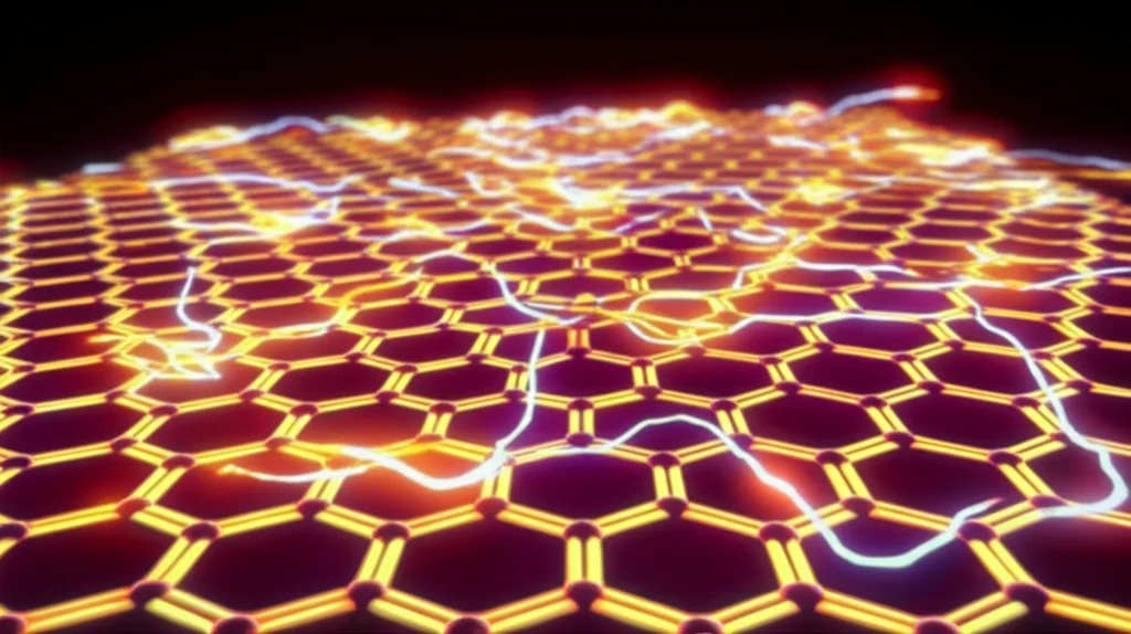
This is where our new heroes, these 2D conjugated coordination polymers (let’s just call ‘em 2D c-CPs for short, shall we?), strut onto the stage. Imagine incredibly thin sheets, maybe just a few atoms thick, where metal atoms (like copper in our Cu3BHT) and organic linker molecules (the BHT part) are arranged in a repeating, highly ordered pattern. The ‘conjugated’ bit is key – it means there’s a system of alternating single and double chemical bonds, which is fantastic for letting electrons zip around easily.
What’s really wild about these 2D c-CPs, and Cu3BHT in particular, is a peculiar combination of properties. They can be excellent electrical conductors, with conductivity values (up to 103 S cm−1) that can rival some metals! Yet, at the same time, they can be pretty poor thermal conductors (below 1 W m−1K−1), more like plastics. This ‘electrical conductor, thermal insulator’ personality is often dubbed the “phonon glass–electron crystal” paradigm, and it’s a dream come true for things like thermoelectric devices (which convert heat to electricity or vice-versa) and, crucially for our story, hot carrier applications! If heat can’t escape quickly from the carriers, maybe they can stay ‘hot’ and mobile for longer? That was the big question.
How We Spied on These Speedy Little Guys
Okay, so we’ve got this super promising material, Cu3BHT. But how do you actually see these hot carriers and measure how fast they’re zipping about? They’re not exactly going to wave for a camera! This is where some seriously cool, ultrafast science comes in. The researchers used a powerful trio of spectroscopic and imaging techniques to map out what happens when light hits these films:
- Time-Resolved Terahertz Spectroscopy (TRTS): This is a bit like giving the material a quick, energetic poke with a laser pulse (the ‘pump’) to create the hot carriers. Then, almost immediately, they ‘tickle’ these carriers with a terahertz (THz) pulse (the ‘probe’). How the THz pulse interacts with the carriers tells us about their conductivity and mobility, essentially how easily they can move, on incredibly short timescales – think picoseconds (that’s a trillionth of a second!).
- Transient Absorption Spectroscopy (TAS): This technique also uses a pump pulse to excite the material. But then, it probes with a broad spectrum of light to see how the material’s absorption of different colors changes as the carriers are generated, move, and eventually cool down. It’s like watching the ‘energy signature’ of the carriers evolve over time.
- Transient Absorption Microscopy (TAM): This one adds a spatial dimension. It maps out where the photoexcited carriers are in the material and how far they spread out (diffuse) over time. Think of it as tracking their tiny footprints as they race across the film.
By combining these sophisticated tools, the scientists could get a really comprehensive picture of the charge transport landscape in Cu3BHT – across time, space, and even different energy levels. It’s like having a multi-dimensional movie of the carriers in action!
The Big Reveal: Record-Breaking Speeds in Two Regimes!
And boy, did Cu3BHT deliver! The experiments unveiled two distinct transport regimes for the charge carriers after the material was zapped with light, and both were pretty mind-blowing for an organic-based system.
First up, in the non-equilibrium regime, right after photoexcitation, it’s all about the hot carriers. These guys exhibited an astonishingly high charge mobility of around 2,000 cm2V–1s–1! To put that in perspective, that’s incredibly fast, especially for an organic material, and it sets new records. These hot carriers were so zippy they could even traverse across the material’s tiny crystal grain boundaries, traveling up to about 300 nanometers, all within a picosecond. Imagine that – crossing multiple city blocks, relatively speaking, in the blink of an eye at the nanoscale!
What’s more, these hot carriers managed to stay ‘hot’ for a relatively long time – up to about 750 femtoseconds (a femtosecond is a quadrillionth of a second!). This might sound ridiculously short to us, but in the ultrafast world of hot carriers, it’s quite respectable, even comparable to some of the best inorganic hot carrier materials like lead-halide perovskites. The researchers also observed something called a ‘hot phonon bottleneck.’ This happens when the hot carriers try to dump their excess energy into the material’s vibrations (phonons), but the phonons themselves get ‘hot’ and can’t dissipate the energy fast enough, effectively slowing down the cooling of the hot carriers. It’s like a traffic jam for energy transfer!
![]()
Then, after these hot carriers cooled down a bit and entered the quasi-equilibrium regime, they became what we call ‘band-edge’ carriers. But even these ‘cooler’ carriers were no slouches! They showed off a remarkable mobility of about 400 cm2V–1s–1 and an intrinsic diffusion length exceeding 1 micrometer. Again, these are fantastic numbers for organic materials, pushing the boundaries of what we thought was possible. Their movement was described as ‘Drude-type, band-like transport,’ which basically means they behaved like well-behaved free carriers moving smoothly through a conductor, rather than hopping awkwardly from site to site, which is common in many less-ordered organic materials.
A Peek at Cu3BHT’s Special Structure
So, what’s the secret sauce in Cu3BHT that allows for such amazing carrier performance? A lot of it comes down to its beautiful and highly ordered structure. The Cu3BHT films were synthesized using a clever liquid-liquid interfacial method, which helps form large-area, thin films (around 20 nm thick) with a nice, smooth surface.
Using incredibly powerful microscopy techniques like aberration-corrected high-resolution transmission electron microscopy (AC-HRTEM) and high-angle annular dark-field scanning transmission electron microscopy (HAADF-STEM), scientists could literally see the atomic arrangement. The copper atoms and the BHT organic linkers form a high-symmetry, non-distorted ‘kagome’ lattice – a sort of hexagonal, honeycomb-like pattern. This dense, conjugated plane is like a superhighway for electrons. X-ray scattering techniques (GIWAXS) further showed that these 2D layers tend to stack in a ‘face-on’ orientation with a tiny interlayer distance of 3.4 Ångstroms.
It’s this combination of in-plane conjugation for easy electron movement and the specific stacking of the 2D layers that likely contributes to its impressive electronic properties. Interestingly, the study notes that while these thin films are semiconducting, thicker bulk crystals of Cu3BHT can actually be metallic. This suggests that the way these thin films are grown, with highly ordered layers, is crucial for unlocking these high-mobility hot carrier phenomena.
What’s Next? The Future is Bright (and Hot!)
Discovering these high-mobility hot carriers in a 2D conjugated coordination polymer like Cu3BHT is a really big deal. It’s not just a new record; it opens up a whole new avenue for developing advanced organic-based optoelectronic applications. Think about it:
- Hot electron transistors: Devices where hot carriers could zip across active regions almost ballistically, leading to incredibly fast switching speeds.
- More efficient hot carrier photovoltaics: Solar cells that could actually harness the excess kinetic energy of hot carriers before it’s lost as heat, potentially boosting their voltage and current output significantly.
- Novel plasmonic photocatalysis: Using the non-equilibrium nature of hot carriers to drive chemical reactions that are difficult or impossible under normal equilibrium conditions.
And the beauty of these 2D c-CPs is their tunability. Scientists can play around with different metal atoms, design new organic linker molecules, and even introduce guest molecules to tweak and optimize their properties. With recent breakthroughs in fabricating large crystals and ultrasmooth films suitable for device integration, the path from discovery to application looks promising.
Honestly, these findings are just scratching the surface. We’re looking at a versatile platform that could lead to a new generation of organic-based electronics. It’s a super exciting time to be watching this space – who knows what other amazing properties these materials are hiding!
This work really highlights how much there is still to explore at the intersection of chemistry and materials science. It’s a testament to the power of rational material design and sophisticated characterization techniques.
Source: Nature Materials